Expert Review: A PSRR-Enhanced Fast-Response Inverter-Based LDO for Mobile Devices
PSRR-Enhanced, Fast-Response Inverter-Based LDO for Mobile, IoT & HPC (28-nm CMOS)
Low-dropout (LDO) regulators are foundational to power integrity in mobile SoCs, IoT nodes, and HPC/AI accelerators. As processes push into sub-10 nm, architects need energy-efficient, compact, noise-resilient regulators with robust transient behavior.
🔍 Why LDO Design Is Critical in Modern Electronics
LDOs deliver clean, regulated rails close to the point-of-load, eliminating switching ripple where PSRR and fast transient response are paramount.
Where They Matter Most
- Mobile processors & battery devices: stable regulation improves efficiency and battery life in phones, wearables, tablets.
- AI accelerators & HPC: low-noise rails and sub-µs transients sustain performance in GPUs/NPUs and data-center silicon.
- 5G & automotive: base stations and ADAS rely on high-PSRR regulators that remain stable under extreme conditions.
📈 Key Contributions of the Proposed LDO Design
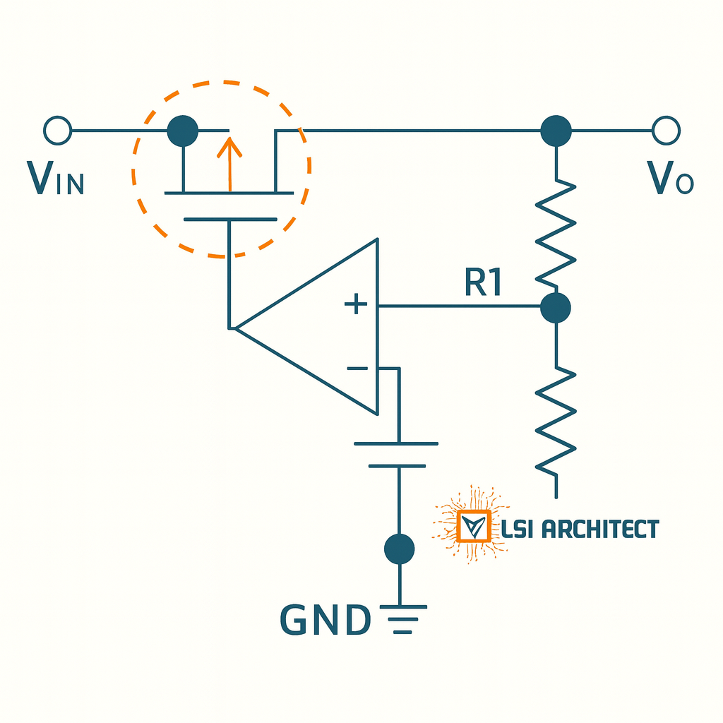
1) Inverter-Based Amplifier for Superior PSRR Core Idea
- Inverter-based loop sidesteps headroom limits common to classic error amplifiers.
- A non-inverting auxiliary amplifier (AUX) boosts PSRR, suppressing supply ripple that couples into the output.
2) Wide Voltage Operation for Mobile & IoT
- VIN: 0.4 V → 1.1 V
- VOUT: 0.2 V → 1.05 V
- Optimized for low-power processors and duty-cycled IoT systems.
3) Industry-Leading Fast Transient Response
Settling: 71.8 ns (50 mV overshoot), 63 ns (47 mV undershoot)
Overshoot: 81 mV @ 269 ns, Undershoot: 84 mV @ 182 ns
4) Power Supply Rejection Ratio (PSRR)
- 44.3 dB @ 100 kHz, 25.0 dB @ 10 MHz (VIN = 1 V)
- > 30 dB PSRR up to 600 kHz (VIN = 0.6 V)
5) Compact Silicon Footprint for SoCs
- 28-nm CMOS, area 0.023 mm² — ideal for dense multi-rail integration.
🚀 Strengths & Industry Relevance
- Advanced Architecture: Inverter-based control with AUX enhancement raises the PSRR ceiling.
- Proven Behavior: Includes both simulation and measured benchmarks.
- Real-World Fit: Suited for battery-powered mobile, IoT, and automotive platforms where quiet rails are critical.
🔎 Areas for Further Research & Optimization
1) Sub-10-nm Scalability
Assess device noise, leakage, and matching as nodes migrate to 7 nm/5 nm; revisit compensation and biasing strategies.
2) Benchmark vs. Digital & Switched-Cap LDOs
Provide apples-to-apples comparisons on efficiency, response time, area, and noise under identical loads.
3) AUX Power Budget
Quantify the auxiliary amplifier’s quiescent and dynamic consumption to maximize end-to-end energy efficiency.
📝 Conclusion — Power Management IC Design
This work demonstrates a cutting-edge inverter-based LDO with excellent PSRR and nanosecond-class transients in 28-nm CMOS, making it a strong candidate for modern mobile and SoC platforms. Continued research into sub-10-nm behavior and system-level energy optimization will further unlock performance for next-gen electronics.
📌 Reference
Lee, J. Lim and J. Han, “A PSRR-Enhanced Fast-Response Inverter-Based LDO for Mobile Devices,” IEEE Transactions on Circuits and Systems II: Express Briefs, vol. 71, no. 6, pp. 3226–3230, Jun. 2024. DOI: 10.1109/TCSII.2024.3357206.
Keywords: Low-Dropout Regulator (LDO), PSRR, fast-response LDO, CMOS PMIC, analog IC design, inverter-based LDO, mobile SoC power.
❓ FAQs
- How does an inverter-based LDO improve PSRR?
- By leveraging high transconductance per bias current and an AUX non-inverting stage that attenuates supply ripple, improving loop gain where PSRR matters.
- Why target 0.4–1.1 V input range?
- It aligns with deeply scaled cores and IoT rails, enabling efficient point-of-load regulation with minimal headroom.
- What limits transient response in practice?
- Output capacitance, pass-device gm, loop bandwidth, and compensation strategy; careful pole-zero placement and strong gm help achieve sub-100 ns settling.
FAQs
AI is enabling smarter design workflows by optimizing performance, predicting failures, and making real-time adjustments for enhanced reliability.
Industries like consumer electronics, IoT, and medical devices see significant advantages from ultra-low-power and energy-harvesting analog ICs.
Miniaturization supports the growing demand for compact, high-performance devices like wearables, IoT sensors, and portable medical equipment.
Analog ICs, such as RF amplifiers and mixers, play a critical role in ensuring high-frequency performance for ultra-fast communication systems.
Meta Description:
Discover the top trends in analog IC design for 2025, including AI integration, energy-efficient designs, and sustainability. Stay ahead in the fast-evolving world of analog circuits.
Conclusion
Analog IC design is at the forefront of technological innovation, driving advancements across industries. Trends like AI integration, energy-efficient designs, and sustainability are shaping the future of this field. By staying ahead of these trends, engineers can create groundbreaking solutions that meet the demands of 2025 and beyond.