The field of CMOS operational amplifier (op-amp) design is advancing rapidly, fueled by the growing demands of IoT devices, biomedical electronics, automotive systems, and high-performance computing. Today’s op-amp innovations focus on ultra-low-power operation, high precision, advanced process technologies, and AI-driven optimization.
1. Current State of the Art in CMOS Op-Amp Design
1.1 Ultra-Low Power & Energy-Efficient Op-Amps
Modern CMOS op-amps achieve nanoamp-level quiescent currents, enabling exceptional battery life for portable and IoT devices:
Texas Instruments TPS7A02 – 25 nA IQ, enabling up to 8.7 years of battery life (vs. 5 years conventional).
Microchip MCP1811 – 250 nA IQ, delivering a 4× battery life extension.
University of Macau (65 nm) – 930 nA IQ with adaptive biasing for dynamic efficiency.
Advanced Biasing Innovations:
Hybrid Biasing Schemes – Combining dynamic and adaptive current control.
Load-Sensing Architectures – Auto-switch between 2-stage and 3-stage configurations.
Subthreshold Operation – Weak-inversion designs for energy harvesting applications.
1.2 Advanced Process Technology Integration
Migration to deep-submicron CMOS nodes enhances power-supply rejection ratio (PSRR), bandwidth, and integration density:
28 nm CMOS – –110 dB PSRR, 25 mV dropout.
65 nm CMOS – >60 dB PSRR up to 10 MHz with feed-forward ripple cancellation.
45 nm CMOS – 30% performance gain, 30% power reduction, 2× density increase.
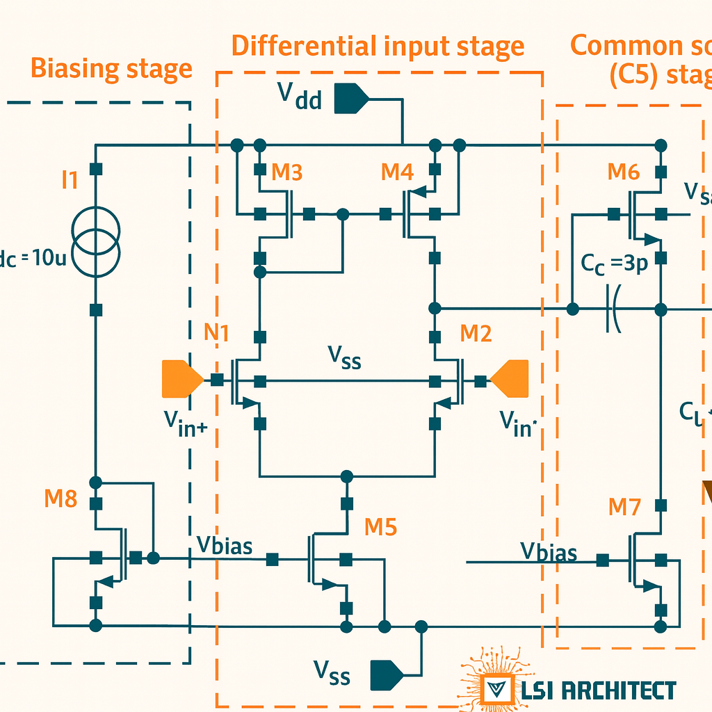
Compensation Techniques:
Nested Miller – Minimal capacitor size for full integration.
Feed-Forward – Eliminates right-half-plane zeros for stability.
VCCS Compensation – Maintains stable zeros independent of load variations.
1.3 Precision & Accuracy Enhancements
To meet the demands of precision analog IC design, engineers are pushing offset, drift, and noise to record lows:
Chopper-Stabilized Architectures – Offset <5 µV; drift <0.1 µV/°C; bias <1 pA; noise <10 nV/√Hz @ 1 kHz.
Zero-Drift Techniques – Offset ≤10 µV; drift 0.05 µV/°C; rail-to-rail operation ±100 mV beyond rails; ultra-low noise 1.1 µVpp (0.01–10 Hz).
1.4 Miniaturization & High-Density Integration
ROHM TLR377GYZ – 0.9 × 0.6 mm WLCSP (69% smaller footprint), 1 mV offset, 12 nV/√Hz noise.
Integration challenges include substrate noise immunity (>60 dB), mixed-signal coexistence, and achieving area <0.01 mm² in 45 nm CMOS.
2.Current Research Directions in CMOS Op-Amp Design
2.1 AI & Machine Learning Integration
ML-Based Design Optimization – Reducing SPICE simulation runs by 56–83%.
Neural Network Spec Predictors – For faster architecture selection.
LLM-Driven Analog IC Synthesis – Accelerating topology exploration.
2.2 Digitally-Assisted Analog Circuits
2.3 Advanced Circuit Topologies
Multi-Stage Architectures – Achieving up to 169 dB gain with active-Miller networks.
Double-Gate MOSFETs – Mitigating short-channel effects.
Capacitor-Less Designs – RIPO structures, push-pull outputs, and feed-forward ripple cancellation.
2.4 Beyond-CMOS & Neuromorphic Approaches
Quantum-Dot Amplifiers – GHz-range parametric gain.
Spiking-Neuron Circuits – Subthreshold operation for neuromorphic computing.
Memristive Synapses – Enabling on-chip learning in analog neural networks.
3.Conclusion
CMOS operational amplifier design is at a transformative stage, merging ultra-low-power performance, precision, AI-driven design, and beyond-CMOS technologies. Future op-amps will integrate neuromorphic features, quantum effects, and digital intelligence, driving innovation in IoT, biomedical devices, automotive electronics, and quantum computing applications.