Analog vs. Digital VLSI Design: Key Differences
Analog vs. Digital VLSI Design: Key Differences (2025)
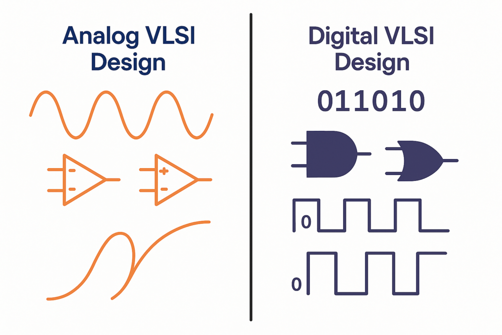
VLSI has enabled compact, high-performance systems. Both analog and digital design are vital—yet they differ in goals, workflows, and where they shine. Use this guide to choose the right approach for your next project.
Continuous vs. Discrete
- Analog VLSI handles continuous phenomena (sound, light, temperature). It focuses on precise amplification, filtering, and conversion.
- Digital VLSI processes discrete levels (0/1). It powers logic, control, storage, and data processing.
Craftsmanship vs. Automation
- Analog: Device-aware, layout-sensitive, and iterative. Noise, parasitics, and mismatch demand hands-on expertise.
- Digital: Standardized, tool-driven flow (RTL → synthesis → P&R → STA). Scales reliably to billions of gates.
Specialized vs. Systematic
- Analog: Cadence Virtuoso, Spectre/LTspice; corners & Monte-Carlo; layout methods (common-centroid, guard rings) to cut distortion, noise, and power.
- Digital: Synopsys Design Compiler / Cadence Genus, Questa/Xcelium, Innovus/ICC2; constraint-driven optimization for speed, area, power.
Precision vs. Throughput
- Analog: Gain, bandwidth, linearity, SNR/THD, offset, PSRR, noise, stability/phase margin.
- Digital: Fmax, timing slack, area, dynamic/leakage power, test coverage, IR/EM sign-off.
Real-World I/O vs. Compute
- Analog: Sensors, AFEs, op-amps, oscillators, ADC/DAC, RF front-ends—telecom, audio, biomedical, power.
- Digital: CPUs/MCUs, DSP/AI accelerators, memories, controllers, ASIC/FPGA logic—consumer, networking, compute.
Real-World Noise vs. Scaling
- Analog: Mismatch, thermal/1/f noise, substrate coupling, PVT drift; stability hinges on careful layout and PEX.
- Digital: Clock distribution, variability at advanced nodes, routing congestion, power integrity, and robust DFT.
| Aspect | Analog VLSI | Digital VLSI |
|---|---|---|
| Signal Domain | Continuous waveforms | Discrete 0/1 logic |
| Main Objective | Fidelity & stability | Throughput & efficiency |
| Flow Maturity | Custom, device/layout-aware | Standardized, tool-driven |
| Key Metrics | Gain, BW, SNR/THD, PSRR, PM | Fmax, power, area, coverage |
| Typical Risks | Offset, drift, oscillations | Timing fails, IR/EM, DRC |
FAQs
AI is enabling smarter design workflows by optimizing performance, predicting failures, and making real-time adjustments for enhanced reliability.
Industries like consumer electronics, IoT, and medical devices see significant advantages from ultra-low-power and energy-harvesting analog ICs.
Miniaturization supports the growing demand for compact, high-performance devices like wearables, IoT sensors, and portable medical equipment.
Analog ICs, such as RF amplifiers and mixers, play a critical role in ensuring high-frequency performance for ultra-fast communication systems.
Meta Description:
Discover the top trends in analog IC design for 2025, including AI integration, energy-efficient designs, and sustainability. Stay ahead in the fast-evolving world of analog circuits.
Conclusion
Analog IC design is at the forefront of technological innovation, driving advancements across industries. Trends like AI integration, energy-efficient designs, and sustainability are shaping the future of this field. By staying ahead of these trends, engineers can create groundbreaking solutions that meet the demands of 2025 and beyond.