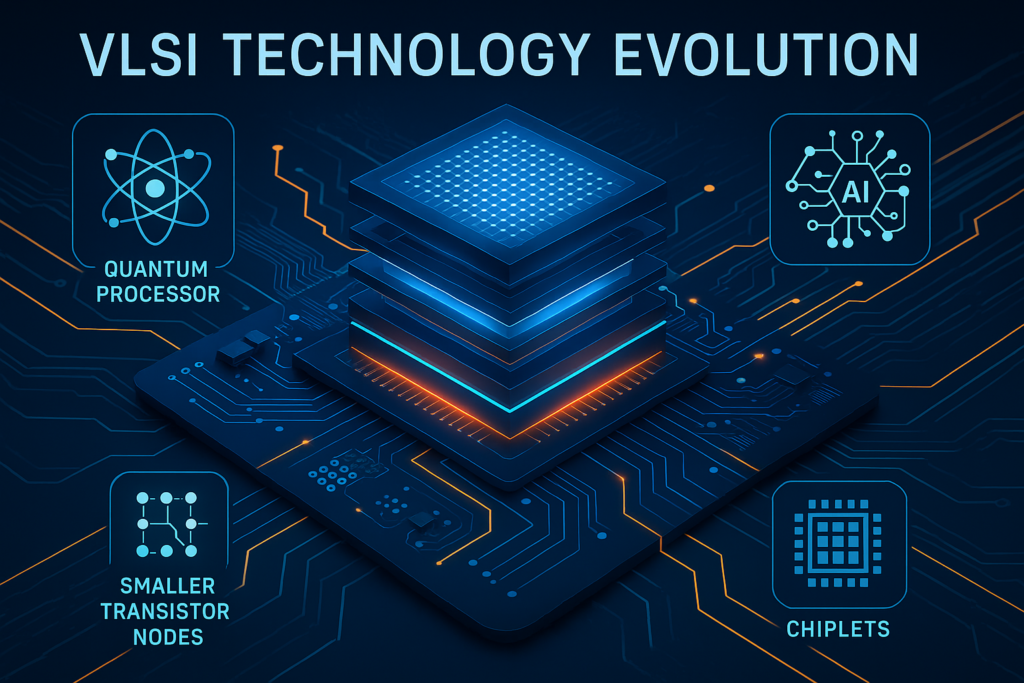
2025 VLSI Design: 12 Data-Backed Trends Shaping Tomorrow’s Silicon

VLSI • Trends • 2025
VLSI is racing toward higher performance, lower power, and denser integration. Here are the trends transforming silicon—from 3 nm & GAAFETs to 3D stacking, chiplets, and AI-driven design—and what they mean for the future of electronics.
Contents
Smaller Nodes & Advanced Processes
3D ICs & Vertical Integration
AI / ML Accelerators
Quantum Computing Interfaces
Chiplet-Based Architectures
Low Power & Energy Efficiency
Analog–Digital Integration
Custom Hardware: FPGA & ASIC
Security & Cryptography in Silicon
AI-Driven Chip Design
Key Takeaways
Conclusion
Smaller Nodes & Advanced Process Technologies
Why it matters: 3–5 nm today and sub-1 nm research tomorrow mean more transistors/mm², higher performance/efficiency, and tighter power budgets.
What’s changing:
Transition from FinFET → GAAFET for improved electrostatics and leakage control.
EUV lithography enables ultra-fine pitches; next up: High-NA EUV.
Beyond-silicon materials (e.g., 2D materials/graphene) under exploration for mobility gains.
KPIs to watch: drive current/ION, IOFF leakage, SRAM bitcell area, BEOL RC delay, energy/operation.
3D ICs (Three-Dimensional Integrated Circuits)
Why it matters: Stacking logic, memory, and sensors shortens interconnects, boosting bandwidth and reducing latency.
Benefits: smaller footprint, higher performance per watt, potential power savings.
Challenges: thermal management, TSV/micro-bump density, heterogeneous design flows.
Use cases: mobile APs, HPC, data centers with tight logic-memory coupling (HBM).
KPIs: bandwidth/stack (GB/s), thermal resistance (°C/W), TSV pitch (µm), yield vs. stack height.
AI & Machine-Learning Accelerators
Why it matters: Massive parallel matrix workloads favor specialized TPUs/GPUs/NPUs and custom ASICs.
What’s trending: tailored memory hierarchies, sparsity support, near-memory compute.
KPIs: TOPS/W, memory bandwidth (GB/s), latency at batch-1, utilization (%).
Quantum Computing Interfaces
Why it matters: CMOS is key for control/readout and cryogenic interfaces in hybrid quantum–classical systems.
Prospects: breakthroughs in cryptography, optimization, materials science.
Hurdles: coherence time, error correction, scalable qubit control.
KPIs: readout fidelity (%), control channel count, cryo power (mW), interconnect latency.
Chiplet-Based Architectures
Why it matters: Modular chiplets cut cost and time-to-market, improve yield, and enable heterogeneous integration.
What’s emerging: mature dies for I/O, compute, AI, analog/RF combined over die-to-die links.
Concerns: standardized interconnects, package yield, multi-vendor security.
KPIs: package yield (%), cost/die vs. monolithic, inter-chiplet latency (ns), bandwidth (GB/s), power/bit (pJ/bit).
Low Power & Energy Efficiency
Why it matters: From phones to hyperscale, performance per watt rules.
Techniques: DVFS, power/clock gating, multi-domain power islands, near-threshold design.
Architectures: ARM momentum in mobile/servers; accelerator offload for efficiency.
KPIs: perf/W (SPEC/GOPS per W), idle/active leakage (µA/MHz), residency in low-power states.
Integration of Analog & Digital Circuits
Why it matters: On-chip ADCs/DACs/RF reduce I/O power and improve signal integrity for comms and sensing.
Benefits: lower latency, reduced board area, higher system reliability.
Care points: noise isolation, substrate coupling, robust power integrity.
KPIs: ENOB/SNDR, phase noise (dBc/Hz), PSRR (dB), jitter (ps), coupling-induced offset (mV).
Customizable Hardware (FPGA & ASIC)
Why it matters: Edge/IoT and data-center offload need task-specific performance and efficiency.
FPGAs: reconfigurable pipelines, rapid deployment and field updates.
ASICs: peak perf/W for stable, high-volume workloads.
KPIs: LUT/BRAM utilization, compile time, ASIC NRE vs. volume, perf/W advantage over CPU/GPU.
Security & Cryptography in Silicon
Why it matters: Hardware roots of trust harden systems against firmware and side-channel attacks.
Integrations: TRNGs, secure boot, crypto accelerators, TEEs, HSM IP.
Lifecycle focus: provisioning → update → decommission.
KPIs: entropy (bits), side-channel resistance (TVLA), secure boot time (ms), key-management auditability.
AI-Driven Chip Design (AI for EDA)
Why it matters: AI accelerates RTL→GDS by optimizing PPA, spotting DRC hotspots, and proposing architectures.
Where it helps: macro placement/floorplanning, routing heuristics, test generation, coverage closure.
Future: AI-co-designed micro-architectures beyond conventional heuristics.
KPIs: closure iterations ↓, WNS/TNS improvement (ps), DRCs/run ↓, coverage hours ↓, tape-out cycle time ↓.
Quick Comparison: Trends, Risks, and Metrics
| Trend | Primary Benefit | Top Risk / Constraint | Metrics to Track |
|---|---|---|---|
| Advanced nodes (GAAFET) | Perf/area, leakage ↓ | BEOL RC, variability | ION/IOFF, SRAM area, energy/op |
| 3D ICs | Bandwidth ↑, latency ↓ | Thermals, yield | GB/s/stack, °C/W, TSV pitch |
| AI accelerators | TOPS/W ↑ | Memory wall | TOPS/W, BW, batch-1 latency |
| Quantum interfaces | New compute domains | Coherence, control scale | Fidelity, cryo power, latency |
| Chiplets | Cost/yield, mix-and-match IP | D2D standards, pkg yield | pJ/bit, ns latency, yield |
| Low power | Perf/W, battery life | Verification complexity | Perf/W, leakage, residency |
| Analog-digital | SI/PI, latency | Substrate noise | ENOB, PSRR, jitter |
| FPGA/ASIC | Time-to-market vs perf/W | NRE, volume | Utilization, NRE, perf/W |
| Security in silicon | Trust, compliance | Side-channels | Entropy, TVLA, boot ms |
| AI for EDA | Fewer iterations | Reproducibility | WNS/TNS, DRCs/run, cycle time |
Key Take aways
Stack smart: 3D ICs and chiplets will dominate for bandwidth and yield economics.
Power first: Perf/W and leakage control define winners from mobile to hyperscale.
Blend domains: Strong analog–digital integration is a competitive advantage.
Automate wisely: AI-assisted EDA reduces closure time and lifts quality—measure it.
Secure by design: Hardware trust anchors must be planned from day zero.
Conclusion
From GAAFETs and EUV to 3D ICs, chiplets, and AI-first EDA, VLSI is evolving toward denser, greener, and smarter silicon. Expect rapid progress in heterogeneous packaging, secure compute, and quantum-classical integration. The winning stacks will blend advanced nodes, vertical integration, airtight power integrity, and AI-assisted design—with security baked in from the start.


